Market
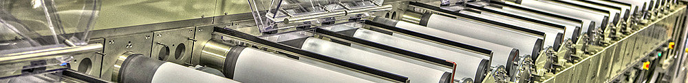
The semiconductor manufacturing process involves two distinct phases, wafer processing, commonly referred to as the front-end, and assembly/test operations which are commonly referred to as the back-end. Besi's equipment is used by customers principally to produce advanced semiconductor assemblies or “packages”. Typically, such assemblies provide the electronic interface and physical connection between a semiconductor device, or “chip” and other electronic components and protect the chip from the external environment.
Semiconductor assembly shares certain common processes but involves three distinct technologies currently depending on the product application required:
Leadframe Assembly
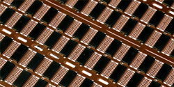
Leadframe assembly, the most traditional approach, involves the electrical connection of the chip via a wire bonding process to a metal leadframe. Leadframe assembly technology is most frequently used to produce semiconductor devices for mass market and consumer electronics applications.
Substrate Assembly
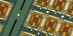
Substrate assembly, an alternative assembly process, has gained increased market acceptance and is used most frequently in new product applications that require high degrees of miniaturization and chip density such as smart phones, tablets and portable personal computers as well as wireless, automotive and cloud based internet applications. In a typical substrate assembly, no metal leadframes are utilized and the electrical connection of the chip is made directly to a multi-layer substrate or through the creation of direct connections to the multi-layer substrate via a flip chip die bonding process.
Wafer Level Packaging
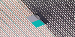
Wafer level packaging, the most advanced assembly technology, eliminates the use of either a metal leadframe or laminated substrate for semiconductor assembly. In wafer level packaging, the electrical connections are directly applied to the chip without the need for an interposer. This process technology enables customers to achieve even higher degrees of miniaturization, chip density and performance and lower energy consumption than substrate assembly but at a higher cost and reduced yield currently. Besi anticipates that wafer level packaging will be more actively utilized for next generation applications such as big data, artificial intelligence and the digital society.
The markets which Besi serves offer significant long-term opportunities for growth particularly in the most advanced packaging applications. Besi is well positioned to capitalize on end-user market opportunities, the most prominent of which include: mobile internet devices (smart phones, wearable internet devices, other wireless devices and logistical systems), intelligent automotive components and sensors, computing (tablets, servers, PCs, flat panel displays, internet applications), data mining, cloud computing and peripherals, the Internet of Everything including the smart management of residential, industrial and municipal equipment and functions, artificial intelligence, virtual and augmented reality, advanced medical equipment and devices, solar, battery and renewable energy applications and LED devices.