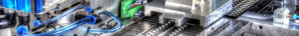
Meco FAP
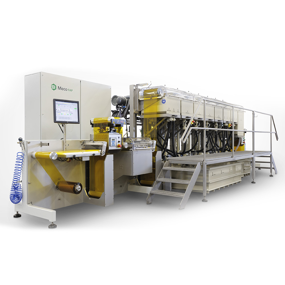
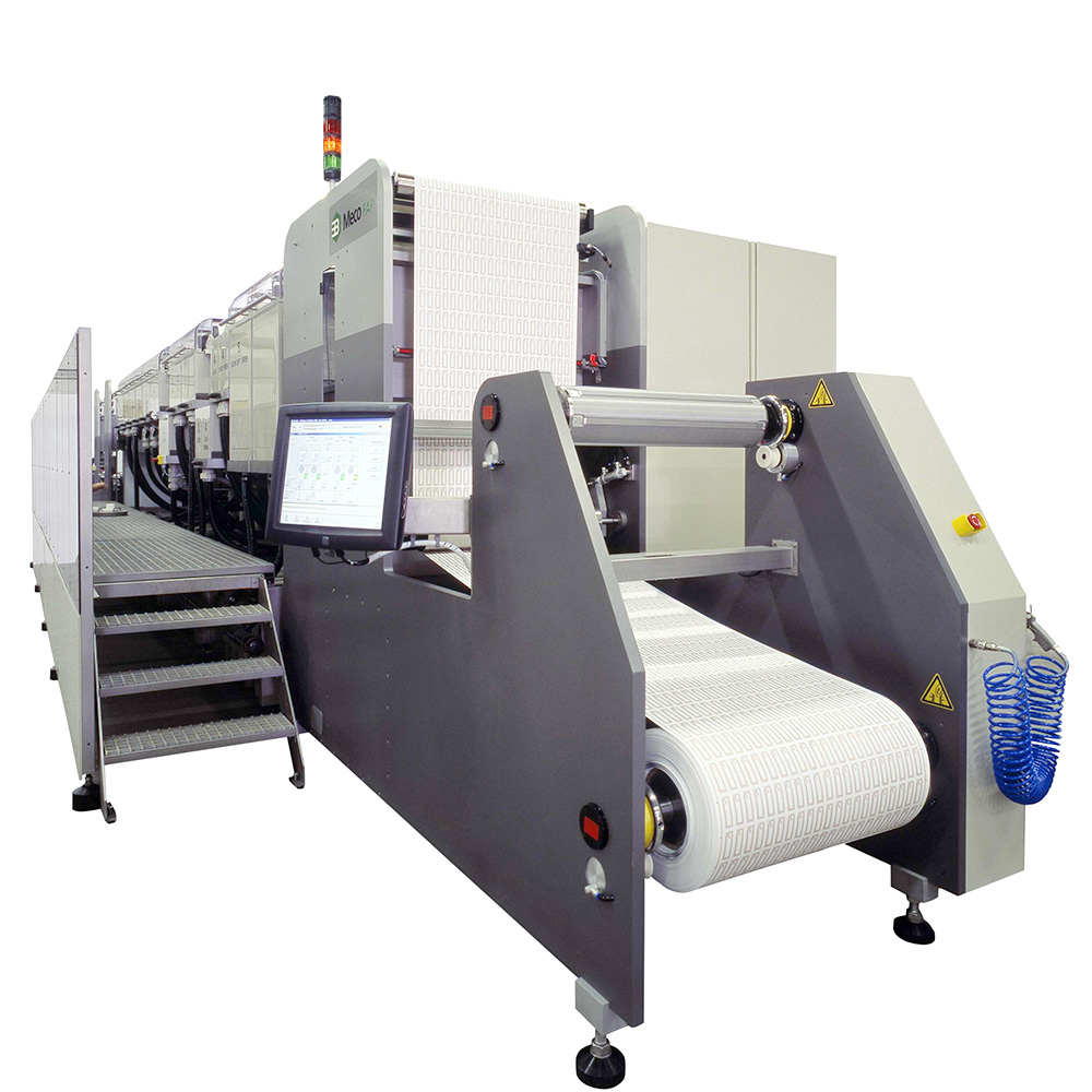
Meco Flex Antenna Plating System (FAP): a unique cost-effective additive process for RFID antenna manufacturing, Flexible PCB and Copper Clad Laminate (CCL).
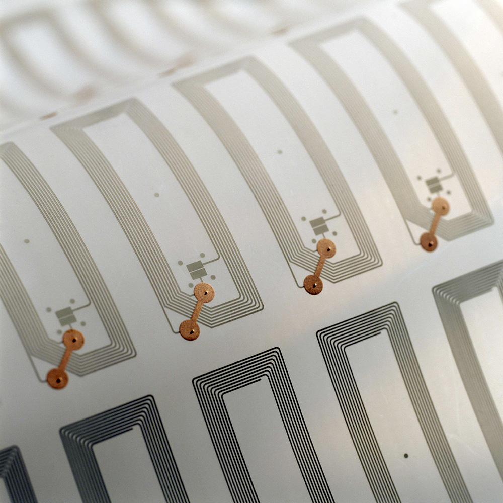
Low Cost RFID Antenna Production
Antenna inlays for RFID passive tags are currently made of etch copper or aluminum. In other cases the antennas are printed using costly conductive ink. Neither production method is meeting the low cost production requirements of high reliability RFID tags.
Additive Copper Process
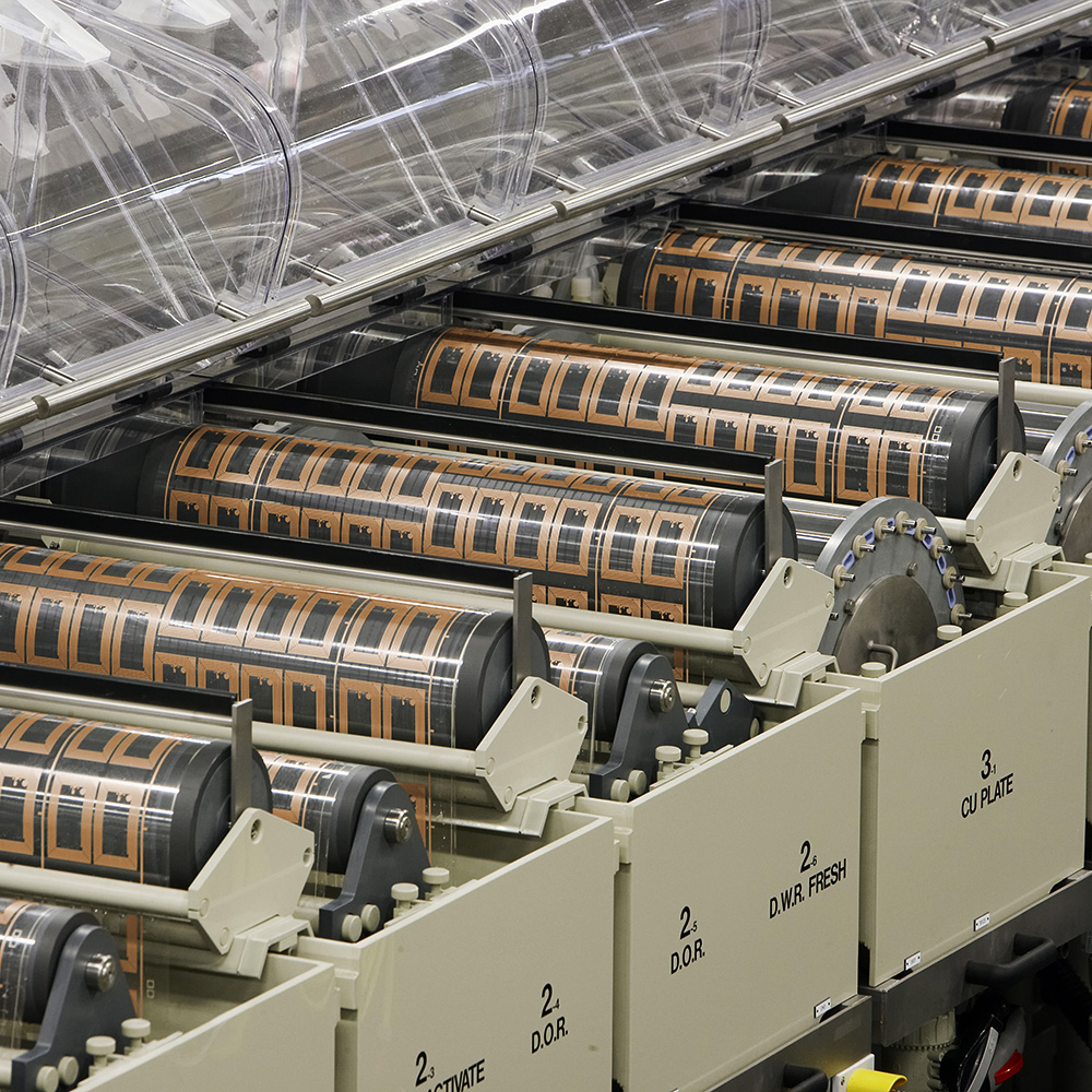
Meco has developed an additive copper process for plating low cost antennas or other components onto flexible substrate. The required pattern should be printed onto the substrate material and then copper is plated on top of it. Contrary to etching processes, copper is only plated where it is actually needed while with etching a lot of copper is subtracted (etched) which leads to waste and a higher cost.
Conductive Ink for Seed Layer Printing
For printing the seed layer pattern a conductive ink (e.g a low-cost non-silver ink) is used. Alternatively the seed layer could also be made using an electroless Nickel-Copper process. The seed layer is only used as a starting layer for the copper plating process. The conductivity is therefore achieved with the plated copper layer.
High Product Flexibility/No Change-Over Time
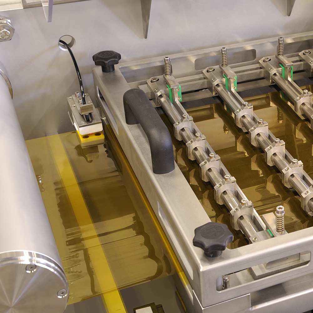
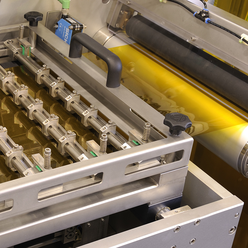
The FAP system can handle a wide range of antenna designs (HF and UHF) or other device structures, without any product related parts resulting in zero downtime when changing over from one design to the other. Depending on the type of antenna, for UHF typically a copper thickness of 2-3 micron is needed while for HF antennas 10-12 micron copper thickness leads to optimum antenna performance.
Specifications
| FAP 330 Ecoline | FAP 430 | FAP 650 | |
|---|---|---|---|
| Substrate width | 330 mm | 430 mm | 650 mm |
| Number of plating drums | 4 | 4 / 8 / 12 / 16 | 4 / 8 / 12 / 16 |
| Web speed | 0.5 - 2 m/min | 0.5 - 12 m/min | 0.5 - 12 m/min |
| Antenna design | HF / UHF | HF / UHF | HF / UHF |
General Input Requirements
- Substrate material: PET, Polyimide, PVC or coated paper
- Substrate thickness: 23 - 150 micron
- Copper plating thickness: 1 - 20 micron
- Surface resistance of seed layer: < 300 mOhm/square
Options
- Strap plating option for HF antenna. This option allows plating on both sides of the substrate in one pass
- For FAP 330 Ecoline: close loop rinsing option. This makes waste water treatment no longer necessary