
Strip Mapping E142 on Esec Die Bonder
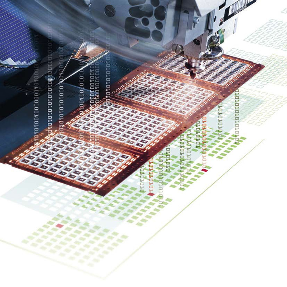
A key to single device traceability - Get ready for the next level of inkless production. IC’s are getting more and more complex, denser, smaller and quality critical with one little lack. By just looking at them you cannot recognize if they are usable or not. That’s where Substrate Mapping E142 comes into play. E142 applies a virtual map like representation of the physical world to a lot of common substrate such as e.g. wafers, strips and trays. Besi Switzerland did implement Strip Mapping based on E142 on the Esec Die Bonder 2100.
Key Features
Strip Identification
- Able to read 2D DataMatrix down to 100 µm dots
- Able to read CODE39 barcode down to 200 µm bars
- Preferred StripID location: Near leading or trailing edge
Strip Mapping E142
- SEMI E142 compliant strip mapping structure
- E142.2 SECS II compliant communication
- Configurable strip map download and upload
- BinCodeMap generation configurable
- TransferMap generation configurable
- Wafer mapping via Stream12 still available
Benefits
Strip Identification
- Only small StripID code area required
- Barcode is sometimes very practicable and easier to attach
- No mechanical contact with code area
Strip Mapping E142
- Well known and widely spread standard
- Works with the same SECS II host you already have
- Customer to select names of map downloads and uploads
- Customer to select level of inkless strip marking (E-Dot ©)
- Linked wafer position to strip position for full single device traceability
- No need to change a proven running system