Datacon 2200 evo plus
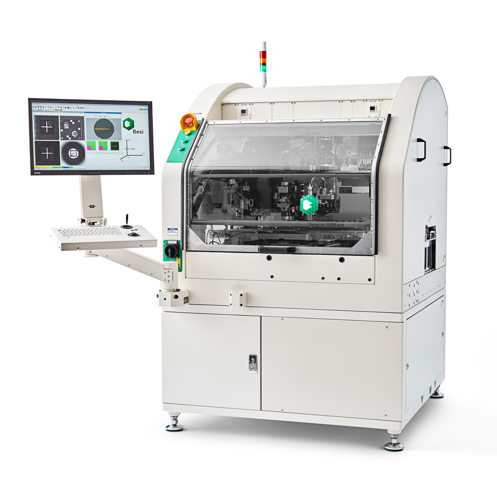
The Datacon 2200 evo plus die bonder for Multi Module Attach assembles all kinds of technologies on a tried-and-tested platform, enhanced with key features for higher bonding accuracy and lower cost-of-ownership.
Besides unbeaten flexibility and full customization possibilities, this evolutionary machine offers higher accuracy with long-term stability using a new camera system and thermal compensation algorithm, higher speed through a new image processing unit, and improved cleanroom capabilities.
Datacon 2200 evo goes PLUS!
-
PLUS accuracy
-
PLUS productivity
-
PLUS flexibility
-
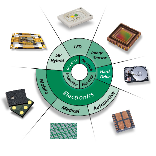
Multi-chip capability
-
Flexibility for customizing
-
Open platform architecture
Key Features
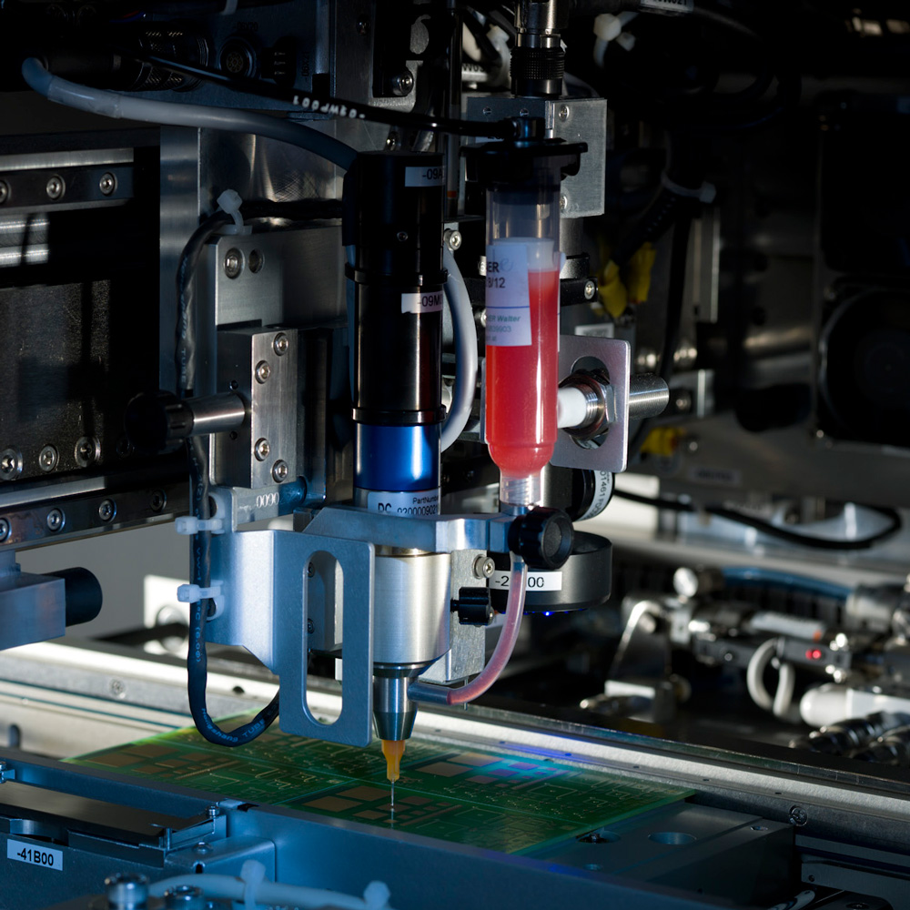
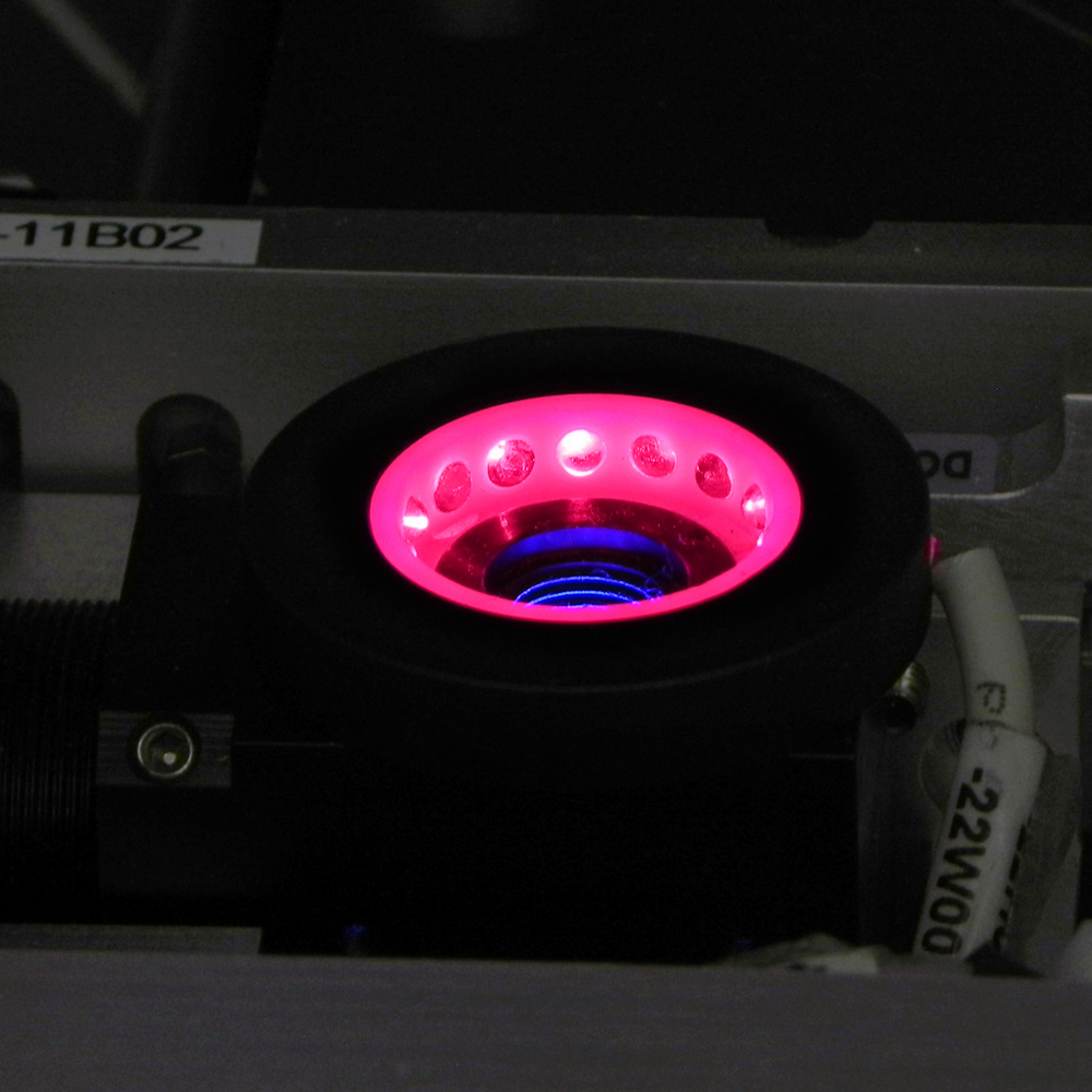
Integrated Dispenser
- Pressure/time (Musashi®), Auger, Jetter types available
- Epoxy stamping option
- Filled and unfilled epoxy, wide viscosity range
- Small footprint, low cost-of-ownership
Vision Alignment
- New high-speed image processing unit
- Full alignment & bad mark search
- Pre-defined fiducial geometry & customized teaching
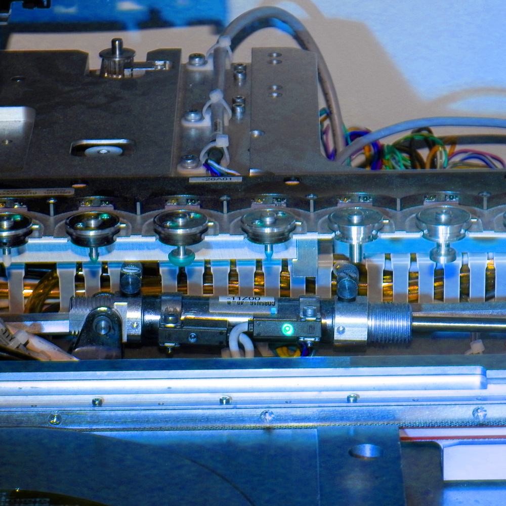
Automatic Wafer and Tool Changer
- Fully automatic cycle for multi-chip production
- Up to 7 pick & place tools (optionally 14), 5 eject tools
- Stamping tools and calibration tools possible
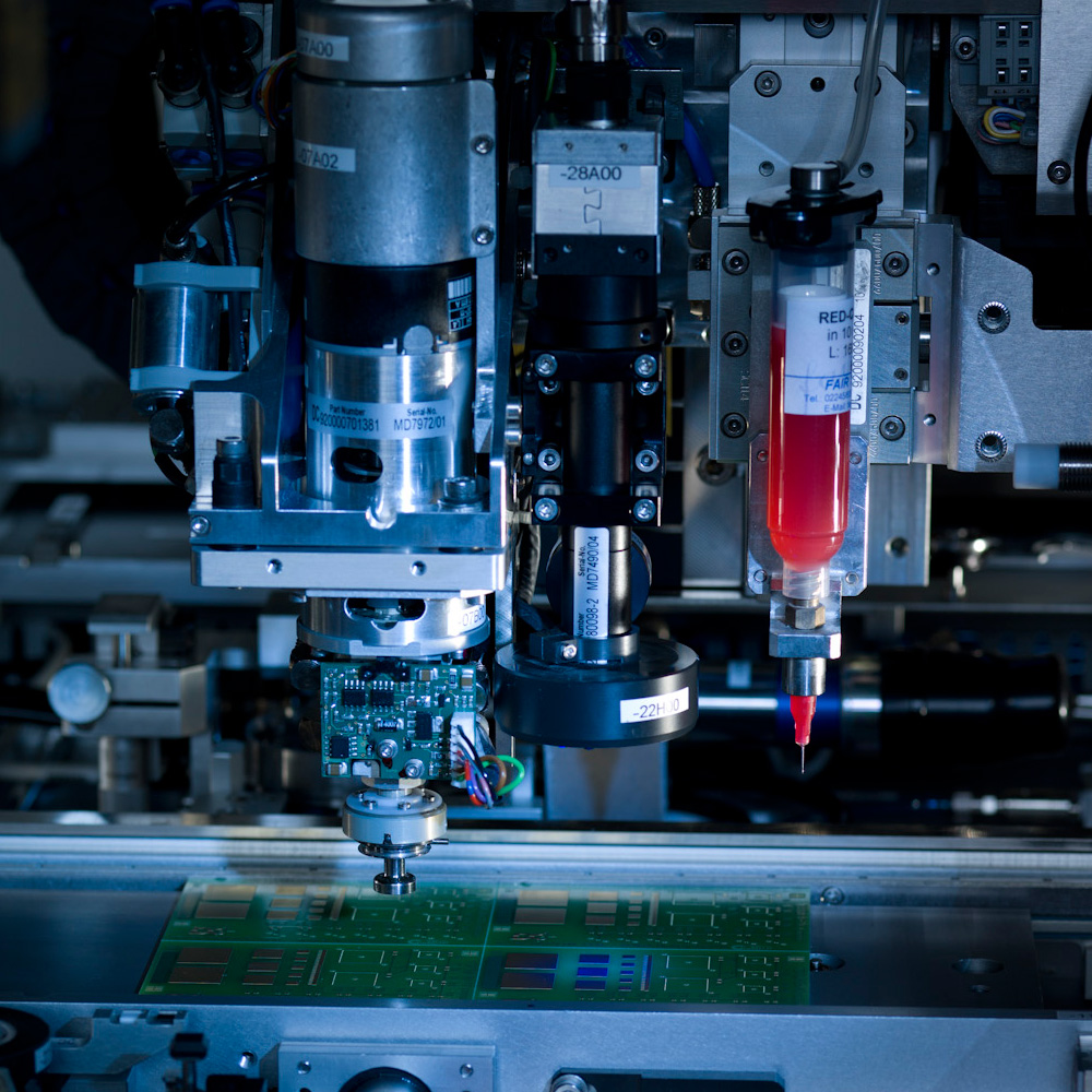
Pick & Place Head
- Die attach, flip chip and multi-chip in one machine
- Die pick from: wafer, waffle pack, Gel-Pak®, feeder
- Die place to: substrate, boat, carrier, PCB, leadframe, wafer
- Hot and cold processes supported: epoxy, soldering, thermo-compression, eutectic
Specifications
Performance
- X/Y placement accuracy: ± 7 µm @ 3s
- Theta placement accuracy: ± 0.10° @ 3s
- Bond Force: 0.5N to 75N programmable
UPH
- Die attach: up to 7,000 UPH/module
- Flip Chip with dipping: up to 2,500 UPH/module
- Flip Chip without dipping: up to 3,200 UPH/module
Bond Heads
- Standard bond head 0° - 360° rotation
- Heated bond head up to 450°C (optional)
- UV Curing (365 nm & 405 nm)
Machine Dimensions
- LxDxH: 1,160 mm x 1,225 mm x 1,750 mm
- Weight: 1,300 kg
Statistics
- Uptime > 98 %
- Yield > 99.95 %
Wafer
- Die size Die Attach: 0.15 mm - 30 mm
- Die size Flip Chip: 0.5 mm - 30 mm
- Die thickness: >50 µm (thinner on request)
- Wafer size: 4" - 12" (SEMI M1)
- Frame size: FF070, FF105, FF108, FF123; automatic change (others on request)
Chip Trays
- Waffle pack / Gel-Pak® 2” x 2” and 4” x 4”
- JEDEC tray on request
Substrates and Carriers
- FR4, ceramic, BGA, flex, boat, lead frame, waffle pack
- Gel-Pak®, JEDEC tray, odd-shape substrates
- Substrate working range: 13” x 8” (325 mm x 200 mm)
Options
- Hardware: Open platform architecture for full customization
- Software: Single component tracking, CAD download, wafer mapping, substrate mapping, barcode scanner, datamatrix recognition and more
Downloads
PDF - 929 KB