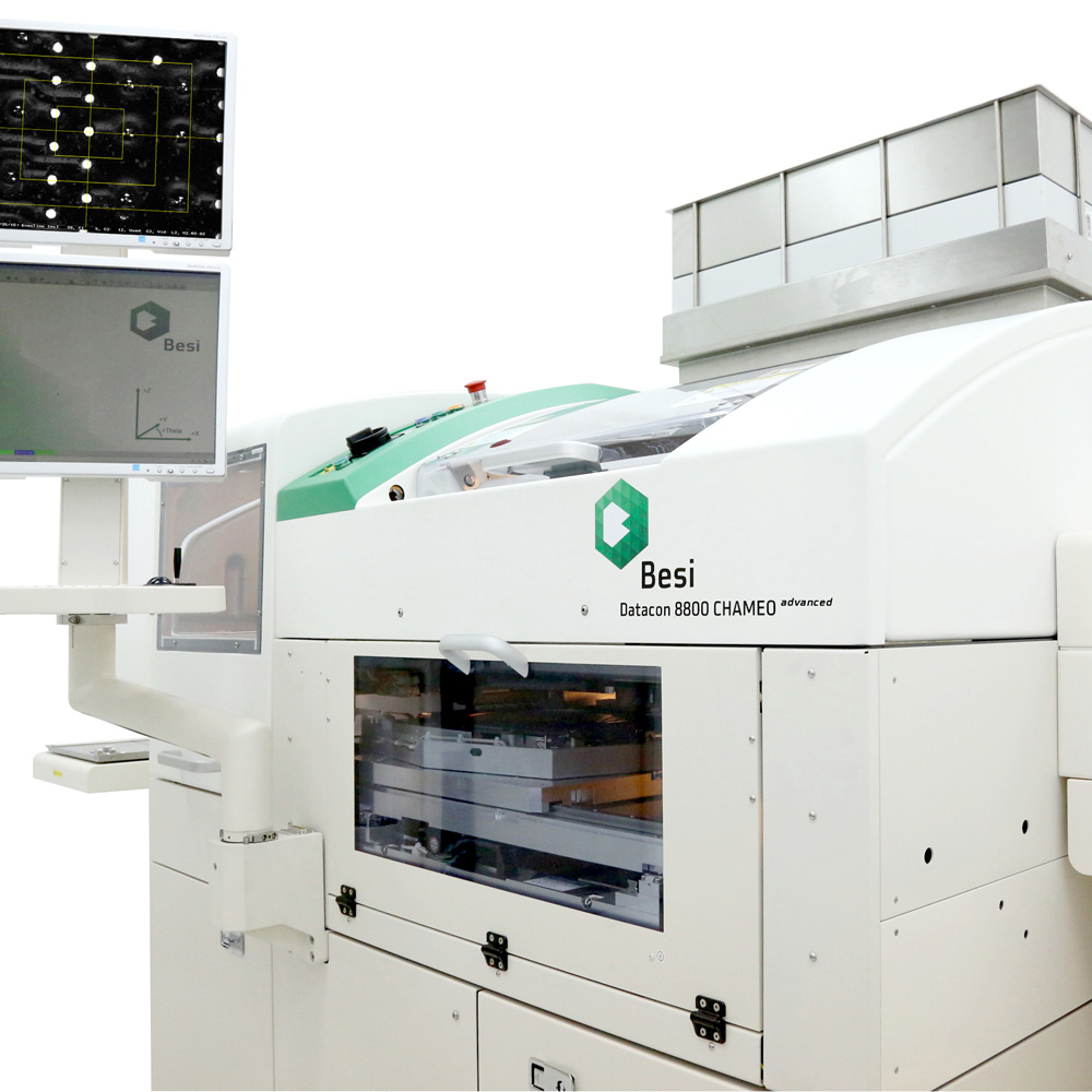
Datacon 8800 CHAMEO advanced

Highest Productivity for FO-WLP
As a new advanced packaging technology, Wafer-Level Fan-Out Packaging (WL-FOP) is a cost effective solution to address increasing demands for performance, form factor, and warpage control.
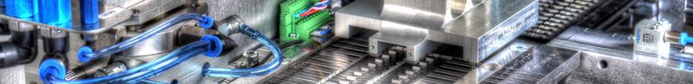
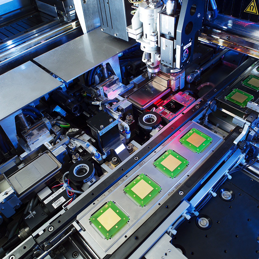
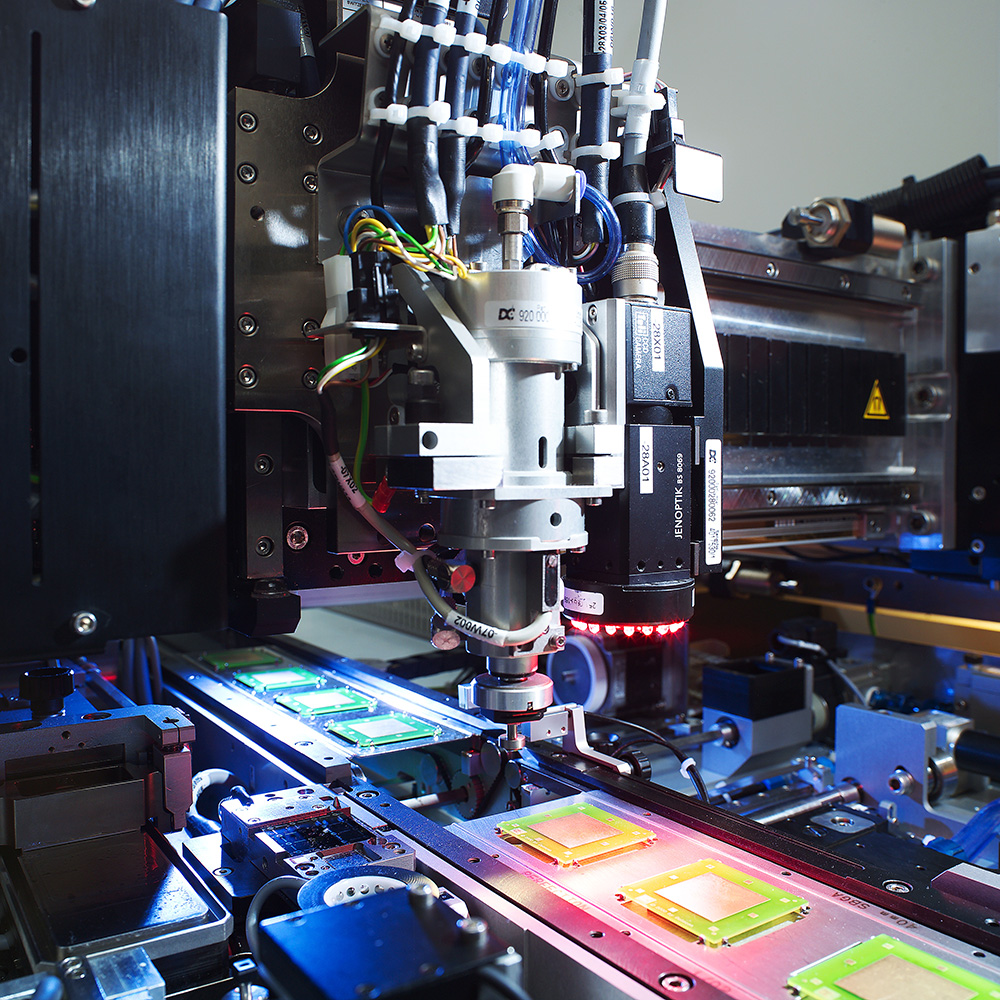
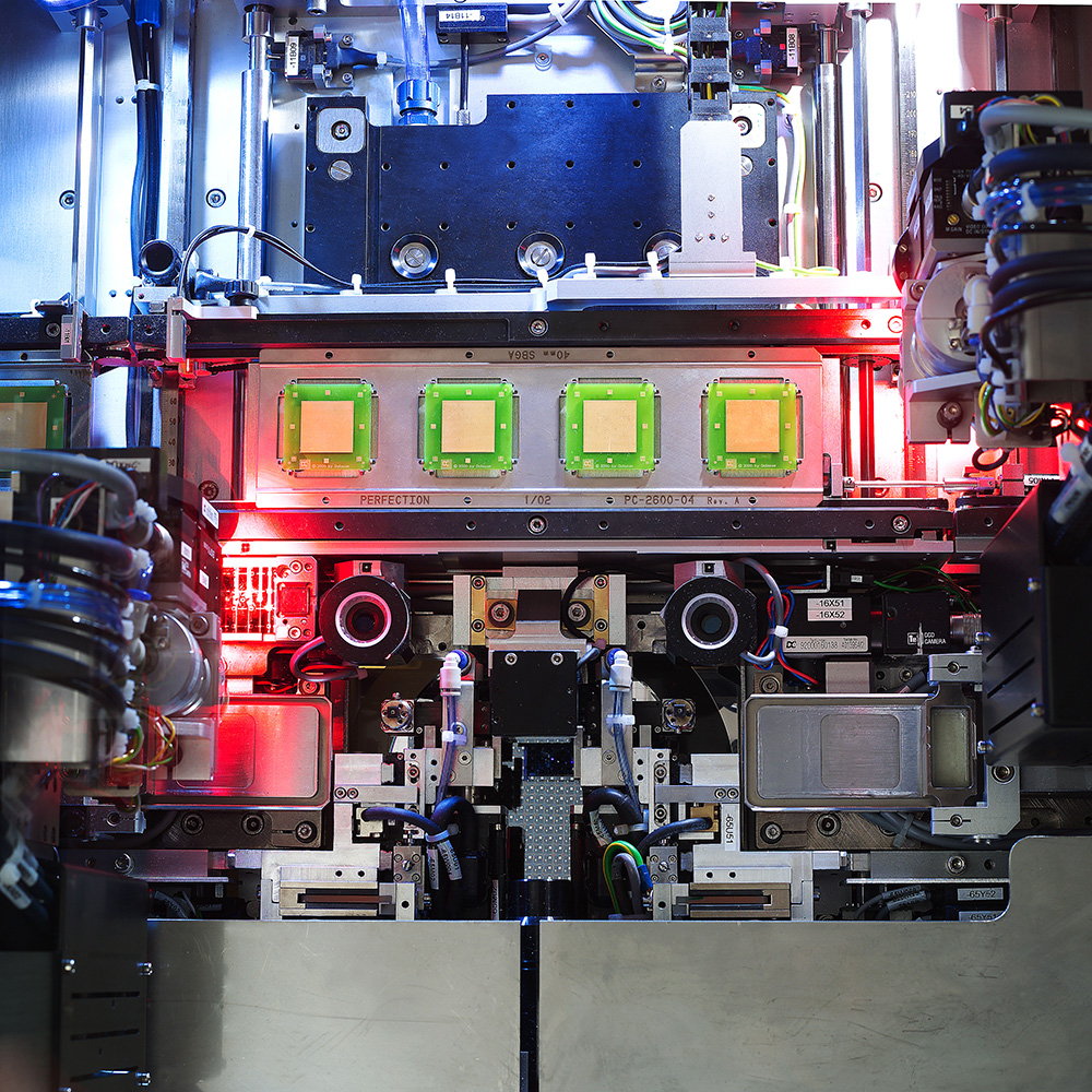
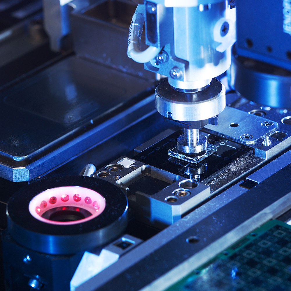
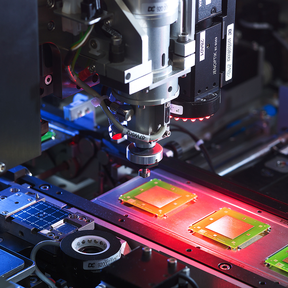
The Datacon 8800 CHAMEO advanced bonder raises a field proven platform concept to an advanced level. It is the perfect fit for chip attach of any WL-FOP process, supporting both face-down (flip mode) and face-up (non flip mode) package designs.
Key Features
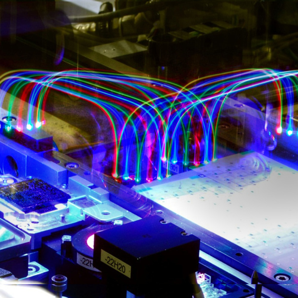
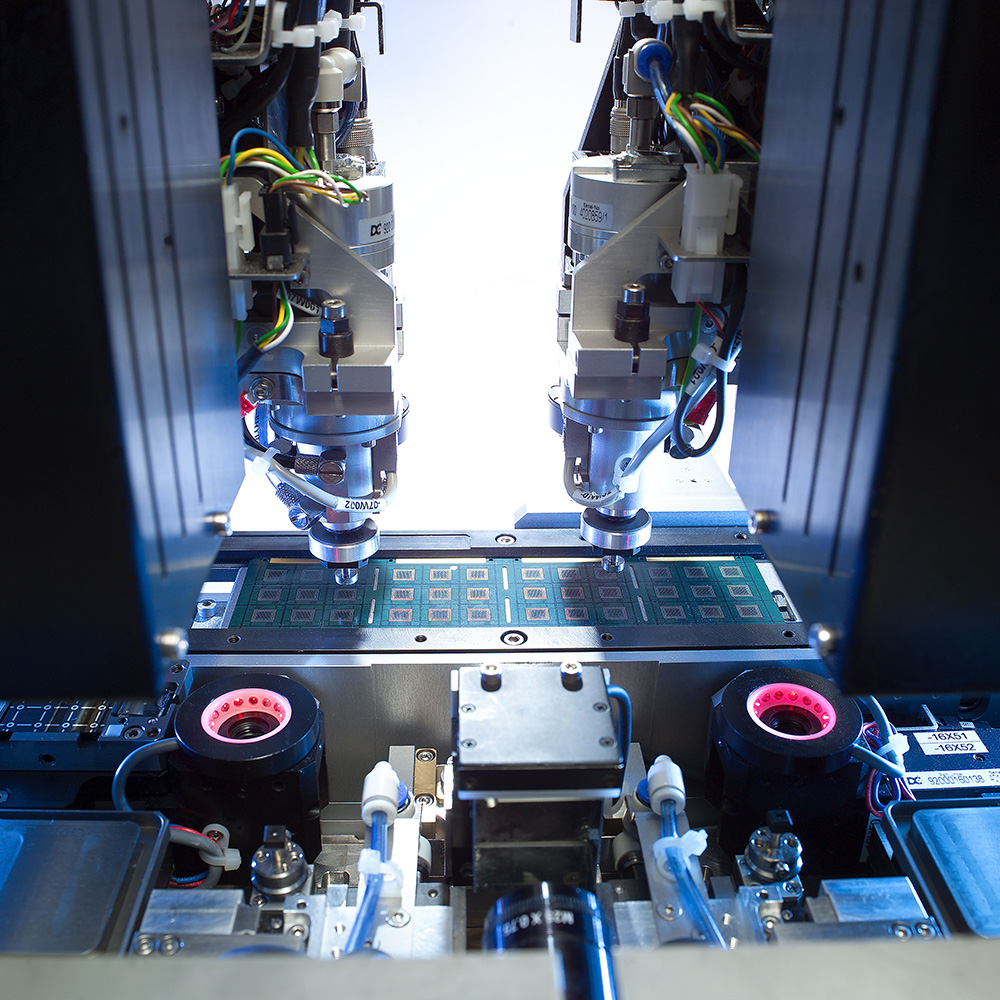
Multi-Chip – Combining Speed, Flexibility and Accuracy
- Multi-chip capability – Flexibility on smallest footprint
- Single pass is king – Improve your Cpk for multi-FC packages
- Waffle pack feeders – Extend your possibilities
- Extra Speed up to +40%
Enhanced Capabilities – Ready for the Future
- Leadframe, strip, boat, wafer – No limits for your substrates
- Customized features – Exactly tailored for your process
- 300 mm / 340 mm Fan Out Wafer Level Packages (FO-WLP) Carrier
- Face-down & Face-up (recipe controlled)
- Clean room class ISO 5
- Foup load port
- Tape & Reel
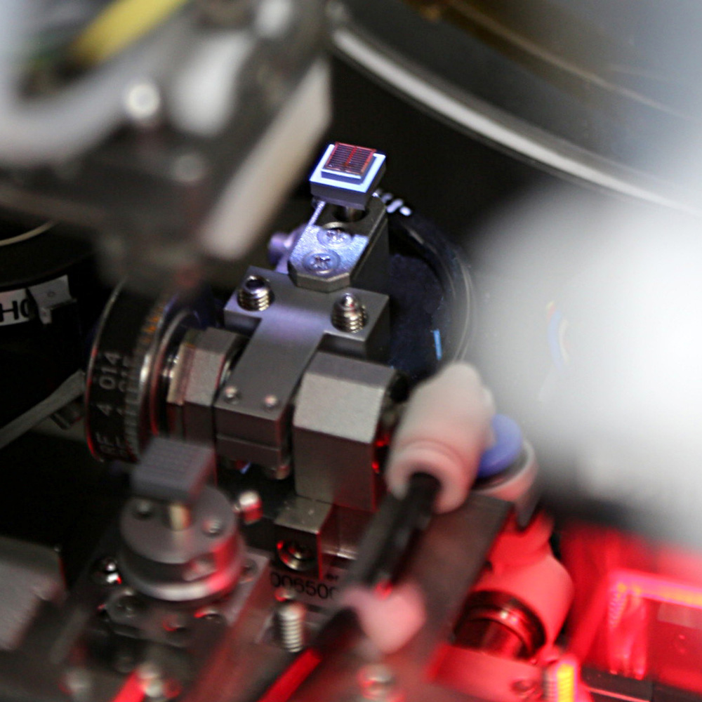
Highest Accuracy – Capturing Tomorrow’s Markets
- Highest Accuracy ± 5 µm / 3 µm @ 3 Sigma
- Local reflow – Mastering sophisticated assemblies
- Long-term stability – Securing high yield at high speed
Wafer Level Applications
- Fan-Out Wafer Level Packages – Highest performance for lowest cost
- Advanced Chip to Wafer – Cost effective dual die stacking
- Through Silicon Vias (TSV) – Entry ticket to the future
Specifications
| X/Y placement accuracy local | ± 3µm @ 3sigma (± 2µm @ 3sigma option) |
|---|---|
| X/Y placement accuracy global | ± 5µm @ 3 sigma |
| Bond force | 2 - 50N (0.5 - 10 N option) |
| Die size face down | 0.3 - 30mm (40mm option) |
| Die size face up | 2.5 - 25mm |
| Die thickness | 50µm - 3mm |
| Wafer size | 8" - 12" (on 8" or 12" wafer frames) |
| Strip, Boats, Panels | Up to 340mm |
| Substrate wafer | 12" |
| Fluxer | option, various cavity plates available |
| Multi Chip | included |
| Tap feeder option | tape size 8 - 32mm |
| Clean room class | ISO5 (option) |
| Footprint | 1,600mm x 1,200mm x 1,880mm (W x D x H) |
| Weight | 2,000kg |
| UPH | Up to 7,000 |
| Vision system | 6 x 6mm FoV for substrate and upwards camera 12 x 12mm FoV for wafer camera |
Downloads
![]() Datacon 8800 CHAMEO advanced.pdf
Datacon 8800 CHAMEO advanced.pdf
PDF - 3 MB